Efforts to combine different high-resolution imaging techniques to provide the most comprehensive material property characterization are on the increase. For example, it is possible to show the structure of a sample with scanning electron microscopy (SEM) and determine its molecular composition with a Raman microscope. As these methods require separate instruments, an inevitable complication is sample transfer and re-identification of the investigated area. Is there a way to dispense with this tedious procedure and replace it with a simple – ideally, one-click – operation?
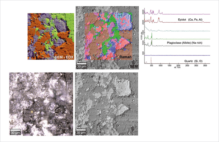
Correlative microscopy involves using two or more microscopy technologies on the same sample area. Over the past decade, the need to describe nanometer-scale samples in full detail has elevated the importance of this combined approach. High-performance analytical techniques relevant to correlative microscopy include, among others, optical microscopy, SEM, atomic force microscopy (AFM), tomography, energy dispersive X-ray (EDX), focused ion beam (FIB) and secondary ion mass spectrometry (SIMS). Linking the data sets enables the correlation of structural, morphological and chemical information, which provides a more detailed understanding of the material investigated. Correlative microscopy may appear advantageous, but it has substantial technical challenges, which makes experiments cumbersome. Moreover, shuttling from one microscope to another may affect the sample’s integrity. However, the primary problem is precise retrieval of a sample’s area of interest, which means you have to rely on fiducial marks or feature recognition. Both procedures are painstaking and time-consuming. Integrating multiple technologies in a single platform to create a hybrid system has been a distinct step in the right direction. For inspecting biological samples, for example, the combination of fluorescence microscopy and SEM has proven useful. In materials science and geology, however, different combinations of optical microscopy with AFM, SEM and EDX are popular. SEM is a very powerful technique for investigating almost any sample that can endure a vacuum environment and it is able to zoom continuously from a field-of-view up to 100 mm in diameter down to a resolution of approximately 1 nm. Despite its extremely high resolution it also has a remarkable depth-of-field, giving images that have great clarity and 3D texture. SEM, however, does not reveal the composition of a sample and, therefore, EDX is often incorporated to identify elemental constituents. Although useful, EDX cannot offer insight into the arrangement and coordination of the detected atoms and their chemical bonds – that particular characterization is best accomplished with Raman spectroscopy. Every compound has a unique Raman spectrum, thus displaying “chemical fingerprints” within the investigated material. This method is non-destructive and doesn’t require labeling or other sample preparation. Although a combination Raman/SEM product was already available, it could only perform Raman measurements at individual points and wasn’t capable of obtaining complete images. The problem with only acquiring a single Raman spectrum is that you never know from exactly which point in the SEM image the spectrum was taken. Even after a flawlessly executed calibration, the focus can move due to thermal drift and charging effects. These effects can easily result in a displacement of 5 µm or more; a distance greater than generally acceptable in correlative studies. However, now we can overlay an image linking measurements precisely and reliably, and this provides an expedient method for alleviating drift.
One day Jaruslav Jiruse, head of R&D at the SEM manufacturer Tescan (Brno, Czech Republic) called me to ask if WITec would participate in developing a “universal SEM” that combined several different analysis techniques with the imaging capabilities of SEM. The potential of Raman in combination with SEM was immediately apparent to me, so I was more than happy to agree to the collaboration (especially given our strong track record in correlative microscopy; for example, our Raman-AFM product was introduced in 2003). In April 2012, we officially began our three-year project (UniverSEM) funded by the EU within the FP7 framework. Russian novelist and historian Aleksandr Solzhenitsyn once said, “The solution is always simple, one must only find it”. His words are so pertinent to research and development – and they made us think carefully about the challenges we were about to face when combining SEM and Raman microscopy. Firstly, during SEM imaging the secondary electrons scattered from the sample are detected by extremely light-sensitive photomultipliers, which are incompatible with the bright lasers required for Raman imaging. Clearly, we could not apply the techniques simultaneously. Secondly, the space inside the chamber and surrounding the SEM column is very limited; SEMs resemble abstract hedgehogs because all the tools orbiting the SEM column aim toward the same point: the sample. This is critically important because the resolution of an optical microscope is directly linked to its numerical aperture – the light cone angle of the objective available for excitation and detection. For a high-resolution objective, this angle is about 140 degrees, leaving precious little real estate for the SEM column itself, much less other detectors. Thirdly, a fully equipped Raman microscope needs several excitation sources (lasers) and spectrometers that weigh more than an SEM chamber’s flanges can support (that is if space was available for attachment, which it isn’t!). We found Solzhenitsyn’s simple solution to the first two problems by placing only the objective and scanner inside the vacuum chamber and changing the scanning procedure – we scan the objective rather than the sample. The location of the objective is offset from the SEM column, freeing space for other detectors. After SEM imaging, the sample is simply transferred to the Raman position using the SEM stage. The numerical aperture of the objective can be optimized as the space above the sample is not shared with other detectors. And you can use a compact scanner because it only has to handle the objective and not samples of varying size and weight. The modular nature of WITec Raman microscopes allowed us to overcome the third and final challenge: excitation sources and spectrometers are coupled to the instrument by flexible optical fibers, meaning that they can be placed far from the SEM chamber whilst always preserving alignment. In a system with “X” mirrors, there will “X” sources of misalignment. Moreover, modern fibers allow very efficient coupling of light, as they are more transparent than air.
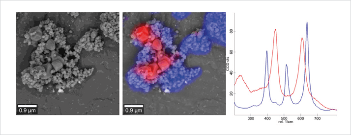
We named the new technology “RISE” (Raman imaging with scanning electron microscopy) and presented it at Analytica 2014 just two years after the project was accepted for funding by the EU. As the SEM and Raman components are essentially two systems using the same vacuum chamber, we didn’t have to make any compromises regarding the respective imaging capabilities. The microscope achieves a lateral resolution of 360 nm and acquires complete Raman images with tens of thousands of data points that can be perfectly superimposed over the SEM image. This is a huge improvement over separate instruments, with shuttling executed at the push of a button and sample orientation preserved consistently. The new microscope enables software-driven quick and convenient switching between Raman imaging and SEM, transformation of the Raman spectra into an image, and the ability to overlay both images to produce a RISE image. To explore and substantiate the capabilities of RISE microscopy we identified and imaged 2D materials, including (but not limited to) graphene and molybdenum disulphide (MoS2), mineral phases in sections of a drilling core, and polymorphs of titanium dioxide (TiO2). We believe that correlative microscopy – exemplified by our RISE technology – will be of great benefit in solving many scientific questions when a single technology is insufficient. Others seem to agree: Photonics Media and the International Society for Optics and Photonics has recognized RISE with their Photonics PRISM Award 2015 as being the preceding year’s most innovative development in metrology instrumentation. And it took a podium spot in The Analytical Scientist’s Innovation Awards in December of the same year (https://theanalyticalscientist.com/issues/1214/return-of-the-tasias/).
Olaf Hollricher is R&D Director at WITec, Ulm, Germany.
Newsletters
Receive the latest analytical science news, personalities, education, and career development – weekly to your inbox.