Introduction
A team of scientists from Helmholtz-Zentrum Berlin für Materialien und Energie GmbH and Plasmetrex GmbH in Germany recently conducted research into the benefits of plasma monitoring of Plasma-enhanced chemical vapor deposition (PECVD) processes using three complementary in-situ monitoring diagnostic tools: Optical Emission Spectroscopy (OES), Mass Spectroscopy and non-linear extended electron dynamics (NEED). During the production of flat panel displays and solar cells two different allotropes of silicon material, hydrogenated amorphous (a-Si:H) and microcrystalline (μc-Si:H) silicon, are commonly deposited using PECVD. Each type of silicon material is typically deposited using gas mixtures of silane (SiH4) and hydrogen (H2), but each with different process conditions. In situ plasma diagnostics reveal parameters such as gas phase composition, electron and ion densities, energy distribution and temperature. All of these parameters influence thin film growth processes and the properties of the resulting thin films.
Instrument Setup
Figure 1a below demonstrates the instrument set up for the researchers and Figure 1b is an image of the OES spectrometer module, an Avantes AvaSpec-ULS2048-2-USB2 dual channel fiber optic spectrometer. The thin film silicon layer deposition was performed in an AKT 1600A cluster tool (Applied Materials) with three process chambers connected to the central transfer chamber. Process gases were introduced into the chambers via a shower head electrode mounted at the top. OES spectra was collected via a fiber optic cable positioned in front of a chamber viewing port.
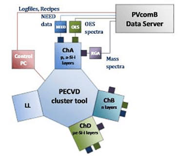 Figure 1a: Experimental setup of PECVD monitoring tool
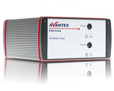 Figure 1b. – Avantes AvaSpec-ULS2048-2-USB2 OES spectrometer
Table 1 below demonstrates wavelengths of spectral line and band transitions of electronically excited atoms, radicals and molecules detected by the Avantes Optical Emission spectrometer

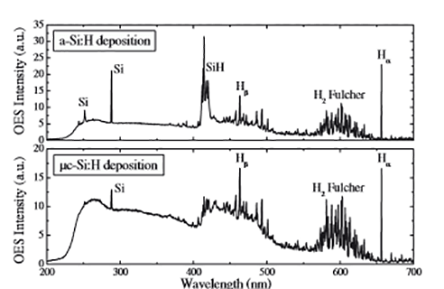
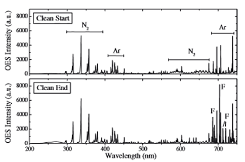
Figure 2 & 3 show some OES spectra obtain during the PECVD process with some notable emission peaks labeled. Figure 2 demonstrates spectra during a si:H and μc-Si:H deposition while Figure 3 shows spectra that can be measured near the end of an Ar/NF3 plasma etch for chamber cleaning. The F peak intensity provides for etch stop detection because at the end of the process F is not consumed by the etching process producing SiF4.
Conclusions
According to the research, PECVD plasma monitoring using spectroscopic OES and other complementary methods provides for rich information which helps to control and optimize thin film deposition processes.
Avantes instruments for OES
Avantes AvaSpec line of instruments is well suited to the Optical Emission Spectroscopy application. The AvaSpec-ULS2048-USB2, AvaSpec-ULS3648-USB2 and new AvaSpec-ULS2048CL-EVO provide for resolution as low as 0.1 nm (FWHM) for resolution of atomic and molecular lines in plasma matrices. Each of these instruments provides for high speed data acquisition as low as 0.6 ms/scan. The instruments are configurable over the range from 200-1100 nm and are available as individual instruments or arrays for multi-point measurements within one or multiple chambers. The new EVO electronics in the AvaSpec-ULS2048CL-EVO provide for high speed USB3 communication, on board data processing and Gigabit Ethernet communication.
>> Download the full Application Note as PDF
Newsletters
Receive the latest pathologist news, personalities, education, and career development – weekly to your inbox.