Raman microscopy solutions for semiconductor research
Latest technological developments bring Raman imaging for semiconductor characterization to a bigger stage
Semiconductors are the foundation of the information age, and their further development is one of the most important endeavors in technology. In the race for new products, the industry requires powerful tools to investigate semiconductor properties and assess the quality of the final product. Discover Raman imaging solutions for detailed semiconductor characterization from the crystals up to the scale of entire wafers.
Correlative Raman Imaging of Compound Semiconductors
This application note demonstrates the use of correlative Raman imaging, photoluminescence and topographic measurements to reveal details of composition and defects in compound semiconductors. It includes the analysis of an entire silicon carbide wafer that reveals its doping, stress, strain, crystallinity and warpage.
DownloadCorrelative Raman Imaging of Semiconducting Materials
The measurements in this application note show the combined approach of Raman microscopy, atomic force microscopy (AFM), scanning electron microscopy (SEM) and second harmonic generation (SHG) microscopy for a detailed characterization of semiconducting materials.
DownloadCorrelative High-resolution Imaging of TMDs
Transition metal dichalcogenides (TMDs) are few- to single-layered materials with unique optical and electronic properties. This study investigated the crystal structure, grain boundaries and strain fields in flakes of molybdenum disulfide (MoS2) using correlative Raman, photoluminescence (PL) and second harmonic generation (SHG) imaging.
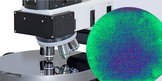
Downloadalpha300 Semiconductor Edition Raman Microscope for Large-area Wafer Inspection
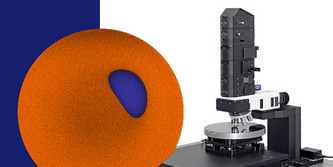
Oxford Instruments WITec’s alpha300 Semiconductor Edition Raman microscope is configured especially for semiconductor research and development. It features active focus stabilization and a large-area scanning stage to allow inspections of wafers up to 300 mm (12 inches).
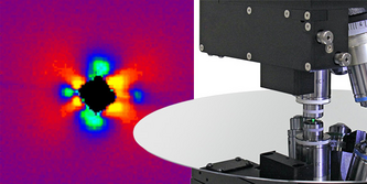
DownloadCutting-edge Cryogenic Raman Microscopy with cryoRaman
This whitepaper describes the applications of cryogenic Raman microscopy for investigations of semiconducting materials. Learn more about the technology and temperature-, polarization- and magnetic field-dependent Raman measurements at temperatures down to 2K.
DownloadFive criteria for high-quality Raman microscopes. An introduction to correlative Raman techniques including application examples
This article provides a comprehensive introduction to Raman imaging. It outlines five key factors to consider when evaluating high-quality instrumentation and describes correlative Raman techniques with supporting application examples.
Download