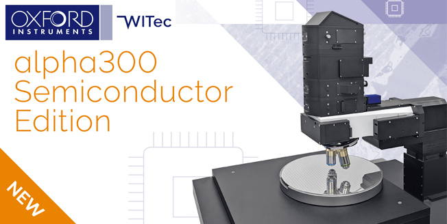
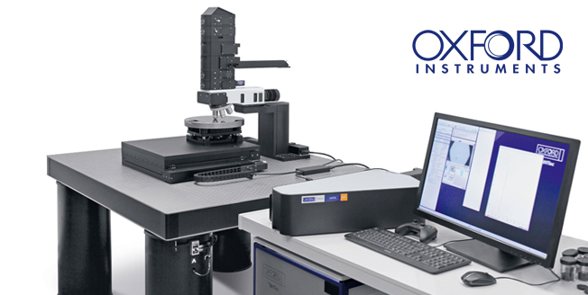
WITec’s alpha300 Semiconductor Edition Raman microscope is configured especially for semiconductor research and development. It features a large-area scanning stage, wafer chuck options, and an advanced workflow manager to streamline measurements.
It also includes: active vibration damping; TrueSurface optical profilometer-driven focus stabilization; comprehensive automation for standardizing measurement procedures and remote operation in controlled environments; and a highly sensitive, on-axis, lens-based, excitation wavelength-optimized UHTS spectrometer.
The first of WITec’s Focus Editions, a line of pre-configured, application-centered systems, the alpha300 Semiconductor Edition is set up to hit the ground running with groups investigating large semiconductor wafers.
Find out more…


