Confocal Raman microscopy is a non-destructive analysis method that is uniquely capable of characterizing semiconducting materials. It can reveal the chemical composition of a sample, identify possible contaminants and even visualize strain fields in 3D volumes. In combination with techniques such as AFM or SEM, semiconducting materials can be investigated more comprehensively.
The Raman principle
The Raman effect is based on the inelastic scattering of light by the molecules of gaseous, liquid or solid materials. The interaction of a molecule with photons causes vibrations of its chemical bonds, leading to specific energy shifts in the scattered light. Thus, any given chemical compound produces a particular Raman spectrum when excited and can be easily identified by this individual “fingerprint.”
Raman spectroscopy is a well-established, label-free and non-destructive method for analyzing the molecular composition of a sample.
Raman imaging
In Raman imaging, a confocal microscope is combined with a spectrometer and a Raman spectrum is recorded at every image pixel. The resulting Raman image visualizes the distribution of the sample’s compounds. Due to the high confocality of WITec Raman systems, volume scans and 3D images can also be generated.
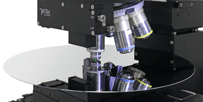
No need for compromises
The Raman effect is extremely weak, so every Raman photon is important for imaging. Therefore WITec Raman imaging systems combine an exceptionally sensitive confocal microscope with an ultra-high throughput spectrometer (UHTS). Precise adjustment of all optical and mechanical elements guarantees the highest resolution, outstanding speed and extraordinary sensitivity - simultaneously!
>> Download the full Application Note as PDF
Newsletters
Receive the latest analytical scientist news, personalities, education, and career development – weekly to your inbox.